






IT News on October 12th: Korean media reported today (local time) that Samsung Electronics is developing several types of NAND flash memory products optimized for artificial intelligence workloads. In addition to the previously announced zNAND-O, there are also zNAND-T and zNAND-I.
The report indicates that the “T” in zNAND-T represents “Throughput” (throughput). This is similar to the HBF concept proposed by Sandisk and SK Hynix, which aims to optimize the read and write bandwidth performance for data center AI semiconductor requirements by using TSV stacked NAND Die.
While the “I” in zNAND-I is an abbreviation for IOPS, which symbolizes random performance, it emphasizes the performance in scenarios involving frequent read and write operations on small amounts of data. The unloading of KV Cache falls into this category of scenarios.
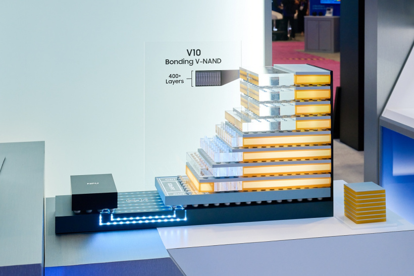
The three zNAND types each have their own specialties, targeting different application loads, indicating that NAND flash memory is shifting from general-purpose products to customized solutions.
Related Reading:
Solid-state drives may be expandable to PB capacity in the future: SK. Hydis introduces its AIN Family product portfolio.