








eBeam Initiative conducted the 15th annual Luminaries survey in July 2026, and announced the results at the annual reception held on September 9 during the period of SPIE Photomask Technology + EUV Lithography Conference. A total of 85 industry insiders participated, representing over 45 companies.
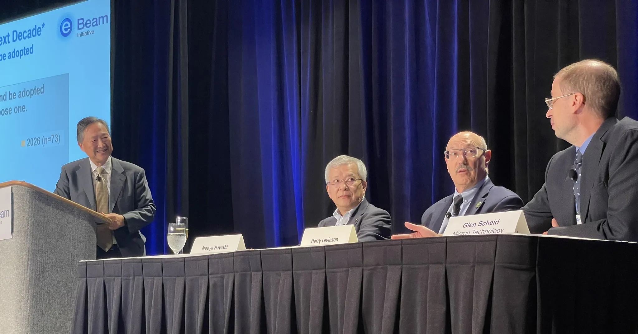
After the annual reception, a panel of experts held discussions based on the survey results, covering topics such as large-sized masks, equipment investment, High - NA EUV, and curved masks. The discussion was chaired by D2S, the CEO, along with eBeam and Initiative, the co-founders, and Aki Fujimura. Participants included HJL Lithography's Harry Levinson, DNP, the honorary researcher, Naoya Hayashi, as well as Glen Scheid from Micron Technology (see Figure 1). This article will report on the key points shared by the group.
eBeam Initiative ( Fujimura ): 66% of industry insiders expect that the industry will adopt large-sized masks in the next decade, with a size of approximately 6 x 12 inches. This survey was completed before TSMC and ASML announced an industry initiative aimed at establishing a 12-inch mask pilot production line by 2031. Why is this shift happening now?
Levinson: The reason on the side of wafer factories is productivity. High - NA EUV These systems are extremely expensive and occupy valuable clean room space. Large-size masks can expose a larger field of view without introducing the complexity of the A/B splicing process, which theoretically can increase productivity by about 40%. Such an advantage becomes very important when each additional system brings with it increased facility and power requirements.
Scheid: The consensus formed around the 12-inch specification is exhilarating. The conversion of mask sizes is extremely rare, and this time there is a clear gain in productivity, which is exactly what the industry needs.
eBeam Initiative ( Fujimura ) : Harry, you were involved in the earlier industry efforts to standardize 9-inch masks. Why is it different this time?
Levinson: The 9-inch proposal was derived based on the historical growth trend of DRAM chip sizes. The target customers did not plan to manufacture such large chips, so this specification did not solve any practical problems and was ultimately rejected. This time, the demand comes directly from chip manufacturers. Intel initiated the discussion, and now TSMC, ASML, and other companies are supporting it. The application scenarios and value are very clear.
eBeam Initiative ( Fujimura ): To achieve the goal of a trial production line by 2031, what needs to be done across the entire supply chain?
Hayashi: The entire ecosystem must be ready at the same time. There is only one supplier for some key links in the mask manufacturing chain. We need to closely monitor the ecosystem and support those links that may impede the availability of the complete process when needed.
Scheid: This is a collective schedule, not a set of independent schedules. The more steps are involved, the lower the overall probability of success. Any delay by a supplier, especially in a single-source step, can slow down the transformation process. Redundancy can reduce risks, but this is a small industry, and the investment scale may be too large to support two suppliers in each category.
Levinson: There are both financial risks and technical risks here. Some tools may require larger platforms and different processing methods, and processes such as uniform etching also deserve closer attention. Financing risks should be addressed as soon as possible, especially for smaller suppliers. Companies planning their wafer factories according to this timeline will worry whether all aspects can be completed on time.
eBeam Initiative ( Fujimura ): What new manufacturing challenges arise when the area of a rectangular mask doubles?
Hayashi: The process based on spin coating will become more challenging. Photoresist coating, development, cleaning, and drying all need to be maintained uniformly on larger rectangular surfaces. Longer edges and corners may cause droplet issues at the corners, therefore these processes require in-depth evaluation.
Levinson: It took about 15 years for EUV's multi-layer film to reach a level suitable for mass production on a large scale. A lot of the experience can be transferred over, but scaling up the size of the multi-layer film blank sheets is not as simple as just installing a few larger machines.
Scheid: The larger the mask area, the greater the chance of particle contamination. According to another survey, contamination and cleaning are indeed one of the main concerns regarding the lifespan of the mask. Large-sized pellicle may be beneficial for wafer factories, but mask manufacturers still need to chemically treat larger surfaces evenly without increasing defects.
eBeam Initiative (Fujimura): Has the question from "whether it will happen" changed to "when it will happen"? High - NA EUV
Levinson: Yes. Just a year ago, people were still wondering whether High-NA really existed. Now it has begun production at Intel, and several companies have also publicly released their roadmaps for it, which represents a significant change. Samsung announced that it will achieve mass production on High-NA in 2028, while TSMC stated that it plans to start using it for large-scale manufacturing in advanced processes from 2030. As for the demand after High-NA, it is less certain. Device and interconnect engineers first need to prove that smaller feature sizes can provide the required performance.
Figure 2: The results of the eBeam Initiative survey in 2026 indicate that equipment procurement will increase over the next three years.
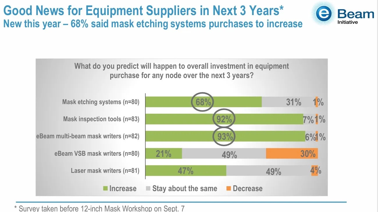
eBeam Initiative ( Fujimura ): 68% of industry insiders expect that purchases of mask etching systems will increase in the next three years (see Figure 2). What are the driving factors behind this result?
Scheid: The procurement of multi-beam writers and inspection tools is expected to increase over the next three years, which reflects both growth in production capacity and the need for additional capabilities. Etching, on the other hand, presents different challenges. The new High-NA mask materials may not be compatible with existing systems and may not be able to operate in parallel with .33 NA materials. Surveys predict that the procurement of etching equipment will also increase over the next three years, but this is more aimed at acquiring new capabilities rather than simply increasing etching production capacity.
Levinson: At the same time, the requirements for uniformity are also becoming stricter. Improving uniformity while introducing new materials has made etching a very active field of research and development.
eBeam Initiative ( Fujimura ): What about the curved wafer target?
Scheid: Curve masking has emerged, thanks to multi-beam writers, and is supported by formats such as MULTIGON. However, it is more difficult to see a solution that automatically generates complete layers for curve wafer targets within a three-year time frame.
Levinson: The advantages demonstrated by curved wafer features are very persuasive, however, backside interconnections and other changes have made the timeline uncertain. On the mask side, curved technology has already arrived and will continue to be enhanced.
Hayashi: Using multi-beam writers to create curved masks is not complicated. Qualification certification remains a challenge, but the level of attention given to this topic at this conference indicates that the industry is making progress in related work.
The conclusion reached by the team at the end is optimistic, but they are not complacent. The productivity logic of large-sized masks is very strong; High-NA has now entered mass production and is also included in the roadmaps of two other companies. Mask factories are investing in new equipment and curved masks. The truly difficult part will be coordinating the entire ecosystem. The industry's history of solving common technical challenges may be its most important advantage as it moves towards 2031.
Reference link:
- 2026 eBeam Initiative Luminaries Survey
- TSMC-ASML large-format mask initiative
- Breaking News by Aki Fujimura from the 12- inch Mask Summit