











On November 13th, according to IT, in the latest episode of the Power On interview program, Bloomberg's Mark Gurman invited Gerard Williams III, former chief architect of Apple, to discuss the current AI trend.
IT's home provides public information. Williams is a chip engineer who has been deeply involved in CPU architecture for decades and is also one of the key figures in Apple's transition from self-developed chips for mobile phones to Mac. He was responsible for the CPU architecture of Apple's A-series and M-series processors and later founded AI, a company specializing in data center chips, advocating for bringing "performance per watt" from mobile devices to the cloud.
In 2019, he left Apple to co-found NUVIA. Later, the company was acquired by Qualcomm, and he led the architecture of Oryon CPU. In 2026, he co-founded another company, NUVACORE.
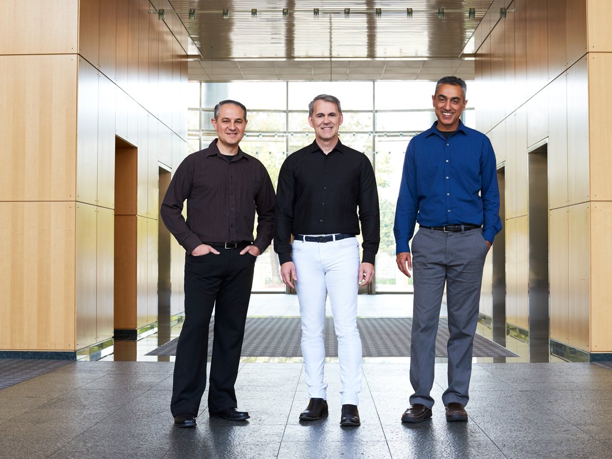
During his time at Apple, he participated in the development of multiple generations of self-developed processors, from A7 to M1. A7 was Apple's first 64-bit mobile processor, while M1 marked a significant shift for Apple, as they transitioned from using Mac chips based on Intel to their own self-developed Apple Sil generation of processors for token issuance. This experience made Williams a representative figure of Apple's approach to "self-developed chips + hardware and software collaboration."
In this interview program, Williams believes that although the entire industry is frantically pursuing NVIDIA's GPU, it is CPU that plays the key role behind the scenes in AI data centers, and its role as the “brain” of CPU is irreplaceable. GPU serves as the “computing power engine” of AI, while CPU acts as the “scheduling center” that ensures the efficient coordination of the entire data center.
Although large language models rely on GPU and AI accelerators to perform large-scale parallel computing, they still require CPU to handle memory scheduling, security mechanisms, operating system operations, and critical serial tasks. The company that created them, NUVACORE, adopts a "core-first" architecture. It does not pre-bind to any particular x86, ARM, or RISC-V instruction sets; instead, it maintains flexibility during the chip core design phase and then optimizes for specific ecosystems later on.
In terms of chip research and development, Williams stated that traditionally, designing a high-performance CPU from scratch usually takes 2.5 to 3 years, with the initial performance modeling and design evaluation phase often taking 7 to 12 months; by utilizing AI tools, NUVACORE has been able to compress this stage to 2 to 3 months.
He compared AI to the “extension of capabilities” for the design team; AI can save engineers a lot of time to experiment with more radical ideas. However, since the models are not always reliable, senior human engineers are still needed to oversee and verify them to ensure the absolute robustness of the chips.
He also stated that the ultimate pursuit of milliwatt-level power consumption in the era of mobile phone chips is becoming a key capability for AI data centers. When designing mobile phone chips back then, engineers had to be extremely meticulous about every milliwatt of power consumption ( milliwatt ) in order to ensure long battery life.
And nowadays, AI data centers consume astonishing amounts of electricity at the gigawatt (Gigawatt) level. If the power-saving technologies used in mobile phones could be applied to servers CPU, the few milliwatts saved per core, multiplied by millions of cores, would allow for 2 to 3 times more computing power to be packed into the same amount of electricity and space constraints.