






IT News on November 7th: According to Reuters, a global race to build the infrastructure for AI is driving billions of dollars into the field of advanced packaging. This once inconspicuous technical aspect has now become a key bottleneck in the production of world-class processors.
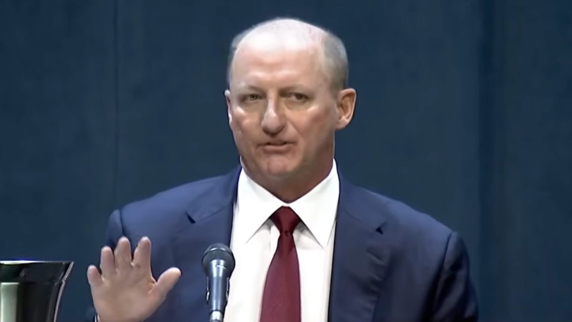
"In the past, packaging was always something you didn't have to worry about at all," Pat Gelsinger, former CEO of Intel and current partner at the venture capital firm Playground Global, recently remarked to the media.
Market research firm Yole Group predicts that the market size of advanced packaging is expected to surpass that of traditional packaging for the first time in 2026, with related capital expenditures expected to approach $28 billion (Note from IT: The current exchange rate is approximately 187.211 billion RMB).
TSMC, the world's largest wafer foundry, dominates the most advanced packaging technologies, including its proprietary wafer-level chip substrate packaging ( CoWoS ). This technology integrates multiple independent silicon chips such as processors and memory on a shared substrate, allowing them to work together at high speeds with extremely high bandwidth.
Currently, this technology has been widely adopted by NVIDIA, AMD, Broadcom, and major cloud giants that have independently developed AI chips. However, TSMC's strained production capacity is forcing chip design manufacturers to seek alternative support.
An industry executive revealed that NVIDIA is providing billions of dollars in financial support to assist Siliconware Precision, a major packaging and testing company under Everlight Technology Group, in expanding its CoWoS packaging capacity.
The executive stated that this previously undisclosed funds will be used to support the expansion of new dust-free factories and the procurement of equipment. In response, NVIDIA did not respond to requests for comments; while Everlight Technology said that they would not comment on market rumors involving their customers.